Time:2025-04-11Reading:958Second
In the semiconductor industry, a microscopic world measured in nanometers, there is an inconspicuous but crucial tool - probes. They are like a doctor's stethoscope, ensuring the health status of each chip through precise "diagnosis".

1、 Nano level precision: the lifeline of chip testing
When the pad size of modern chips shrinks to below 50 microns, equivalent to half the diameter of a human hair, the challenges faced by probes far exceed imagination. According to relevant test data, when the contact position of the probe deviates by more than 0.5 microns, the chip's false measurement rate will soar by 20%. This requires the probe to achieve a positioning accuracy of ± 1 micron, which is equivalent to accurately locating the position of a sesame seed on a standard football field.

2、 Working principle of probe
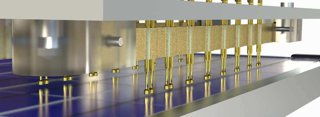
The main tool used for chip testing is semiconductor high-frequency probes, also known as dual head probes. The function of dual head probes is to physically connect with the contact points of the chip through tiny probes after the chip is manufactured, transmit test signals to the inside of the chip, and read feedback data.

This process not only verifies the functionality of the chip, but also detects potential manufacturing defects, ensuring the quality of the final product.
It can be said that every successfully manufactured chip relies on the "precise touch" of the testing probe.

The core of probe technology lies in its extremely high precision and reliability. As the chip manufacturing process continues to shrink, the contact points (i.e. pads or bumps) inside the chip become increasingly small and dense.
This requires the probe to achieve accurate contact within the micrometer range, while having sufficient durability to handle high-frequency testing operations.
For example, on chips with 7nm or even 3nm processes, probes need to make contact in less than 100 microns of space, and the achievement of this accuracy cannot be achieved without the support of high-performance materials and precision manufacturing technology.
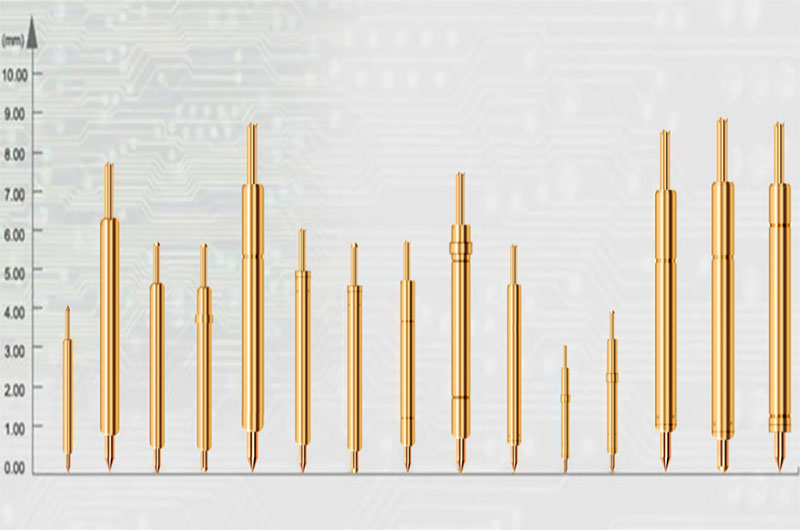
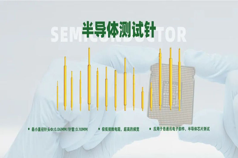
At present, for semiconductor high-frequency needles, Suntory can process the minimum probe diameter: needle tip diameter: 0.06mm/needle tube diameter: 0.10mm.
three、Probe technology
The competition in the field of probe technology is extremely fierce globally. For a long time, companies from countries such as the United States, Japan, and South Korea have firmly held a leading position in the market with their profound accumulation in precision manufacturing and material technology. However, in recent years, Chinese companies have made significant progress in the field of probe technology. useFirst profitFor example, a national high-tech enterprise that has been steadfastly committed to the localization of probes for over 40 years, focusing on the research and development of various testing probes. By adopting advanced material structures, lean coating treatments, and high-quality assembly processes, we provide customers with better testing probe products.For more probe information, welcome to Centalic official website: www.szcentalic.com Learn more!

In the technology war without gunpowder in the semiconductor industry, although probes are small, they are crucial to the overall situation. It is not only the gatekeeper of product quality, but also the witness of technological innovation. In the future, with the development of new technologies such as chiplet, probes will face more complex testing scenarios.