Time:2023-11-25Reading:2277Second
1、 The application of probes in the semiconductor field
Mainly used in semiconductor chip design verification, wafer testing, and finished product testing, it is the core component connecting chips/wafers and testing equipment for signal transmission, playing an important role in quality control of semiconductor products.
1. Wafer testing:
Chip Probing, abbreviated as CP, refers to the use of probes to test the functionality of chips or semiconductor components on wafer products after production and processing, to verify whether they meet product specifications.C
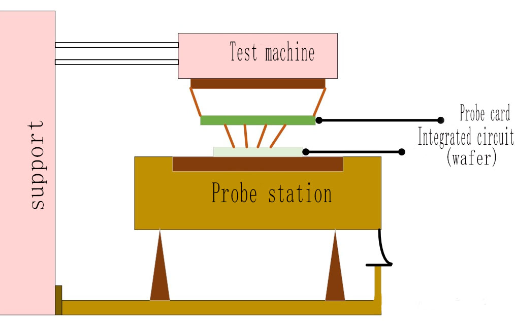 Schematic diagram of wafer testing
The testing process requires the use of a probe station and a testing machine. The probe station automatically transfers the wafer to the testing position one by one, and the pins of the chip are connected to the functional modules of the testing machine through probes and dedicated connection wires. The testing machine applies input signals to the chip and collects output signals to determine whether the chip's function and performance meet the design specifications.

The test results are transmitted to the probe station through the communication interface, and the probe station marks the chip accordingly to form a wafer result mapping, marking invalid chips as much as possible to save packaging costs.
2. Finished product testing:
Final Test, also known as FT or Final Test, refers to the functional and electrical parameter testing of the packaged chip to ensure that the functional and performance indicators of each chip produced meet the design specifications. The testing phase of chip design verification is quite similar to the finished product testing phase.
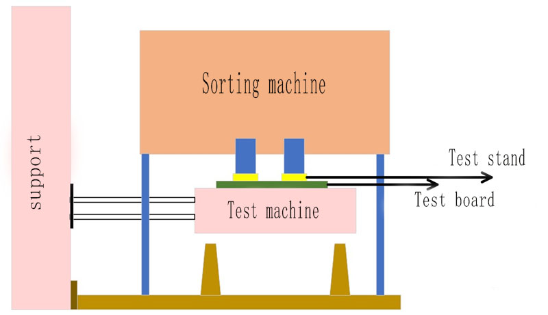
Schematic diagram of finished product testing
The testing process requires the coordination of a sorting machine and a testing machine.
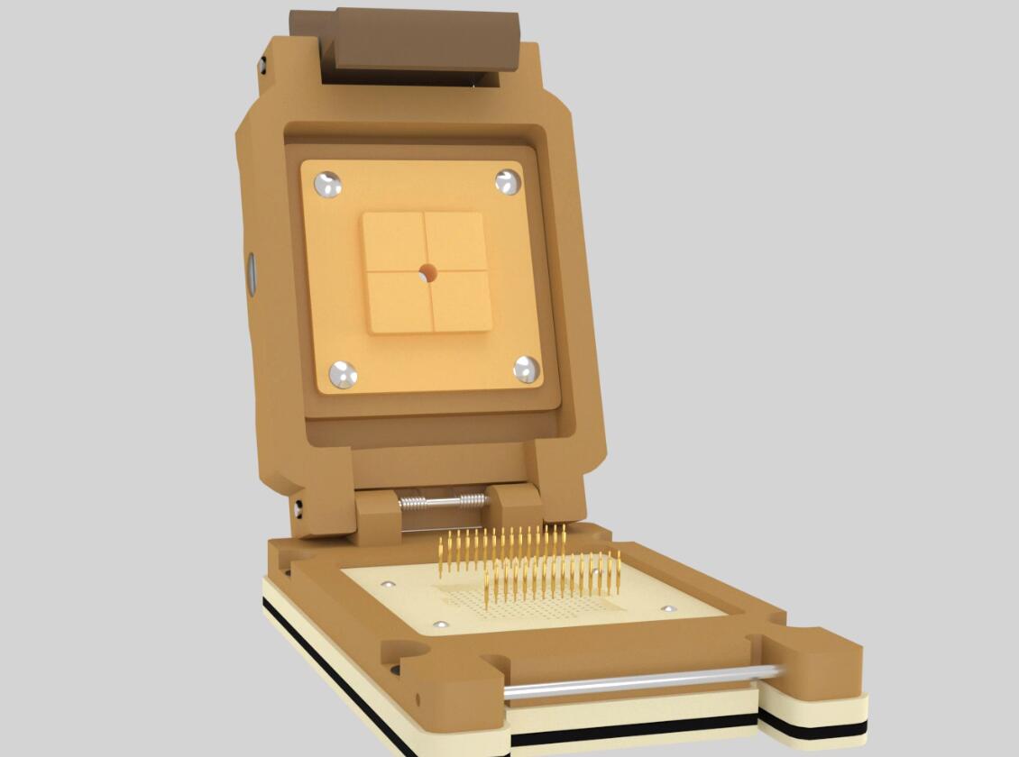
The sorting machine automatically transfers the tested chips one by one to the testing station, and the pins of the tested chips are connected to the functional modules of the testing machine through probes installed on the testing seat.
The testing machine applies input signals to the chip and collects output signals to determine whether the chip's functionality and performance meet the design specifications.
The test results are transmitted to the sorting machine through a communication interface, and the sorting machine marks, sorts, receives or encodes the tested chip based on this.
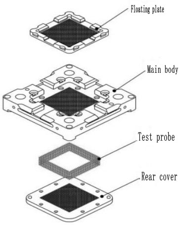
Schematic diagram of test seat structure
2、 Structure and materials of semiconductor testing probes
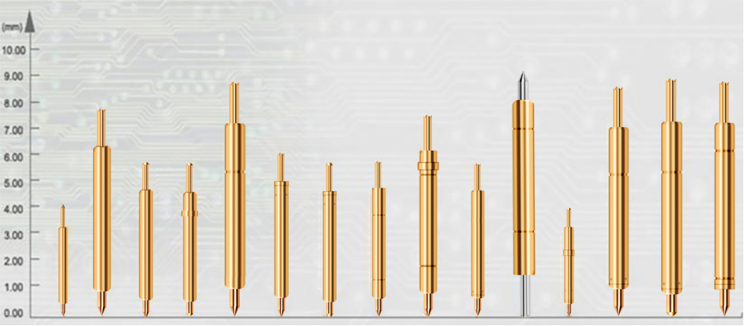
The Centalic semiconductor testing probe is a testing probe composed of three basic structures: a needle, a needle tube, and a spring.
1. Needle: The selection of needle type in the testing environment also directly affects the effectiveness of the test. The needle mainly includes several materials such as brass, phosphor copper, beryllium copper, SK4, etc. Their hardness performance (brass<phosphor copper<beryllium copper<SK4), the higher the hardness, the more wear-resistant the needle is.
2. Needle tube: used for assembling needle rods, equipped with springs inside, mainly made of several materials such as phosphor copper tubes, brass tubes, and white copper tubes.
3. Spring: Installed inside the needle tube to make the probe elastic, mainly made of stainless steel wire and piano wire. Stainless steel wire is the preferred material for probe springs due to its corrosion resistance, high temperature resistance, and resistance to rusting; Qin steel wire has strong elasticity, but is prone to rusting when exposed to moisture, so there is no specific need to use Qin steel wire springs.
