Time:2025-02-21Reading:1631Second
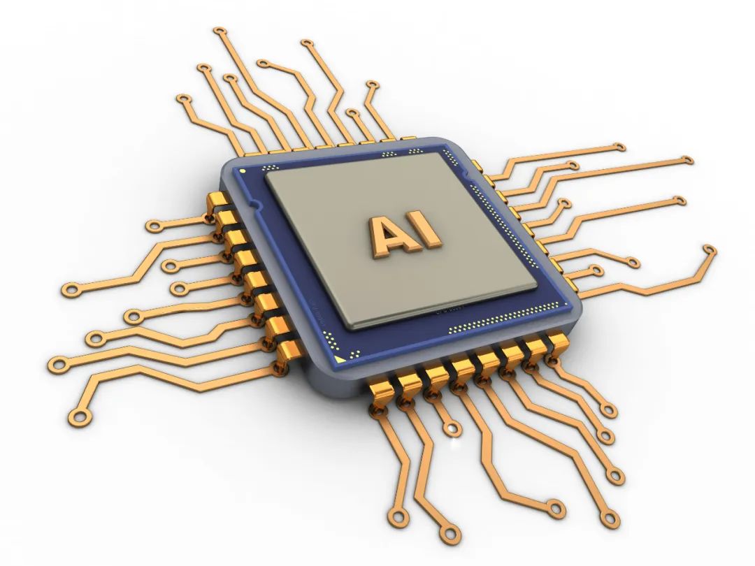
With the rapid development of semiconductor technology, chip as the core carrier of information technology, its performance and quality improvement has become the key to promote scientific and technological progress. However, the chip will inevitably appear aging in the process of long-term use, which directly affects the performance and life of electronic products. Therefore, chip burn-in testing has become a crucial link in the semiconductor industry. This article will delve into the challenges of chip burn-in testing and introduce a semiconductor test probe that can easily break the game.
Chip burn-in test is a process of comprehensive testing and evaluation of chips by simulating the actual working conditions of long-term use and various extreme environments. The goal is to verify the stability and reliability of the chip over long periods of use and in extreme situations. However, there are many challenges to this testing process:
●High test complexity : With the continuous improvement of chip integration, the complexity and difficulty of burn-in test are also increasing. Testers need to simulate various environmental factors, such as high temperature, low temperature, high humidity, etc., to verify the stability of the chip in different environments.
●Long test time : The burn-in test requires a long run to assess the chip's life and performance decay. This not only consumes a lot of time and resources, but also puts extremely high demands on the test equipment and environment.
●High test accuracy : In order to ensure the accuracy of test results, burn-in testing requires high-precision test equipment and probes. Any small error may lead to the deviation of the test results, which will affect the judgment of the chip performance.
Faced with many challenges in chip burn-in testing, a high-performance semiconductor test probe becomes the key to break the problem. With its unique design and excellent performance, this probe has played an important role in the chip burn-in test.

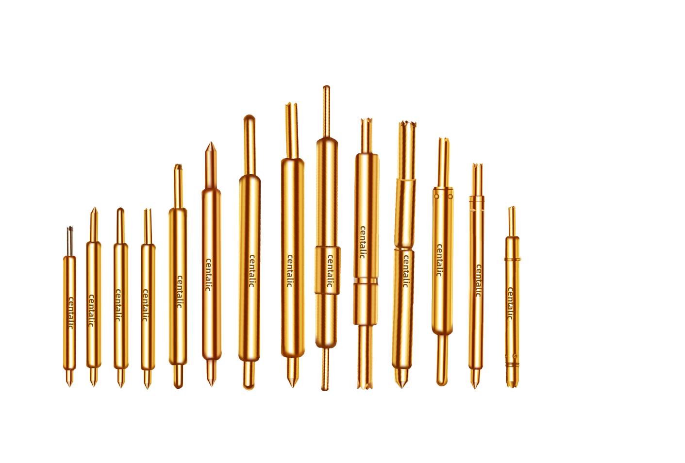
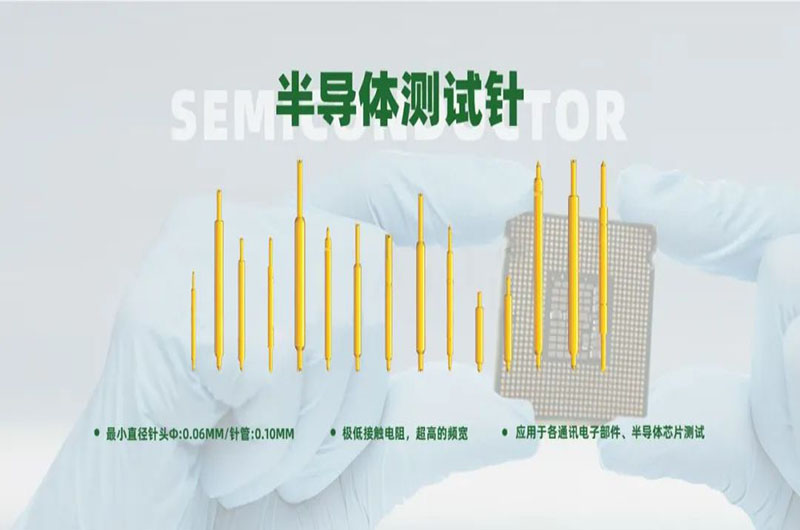
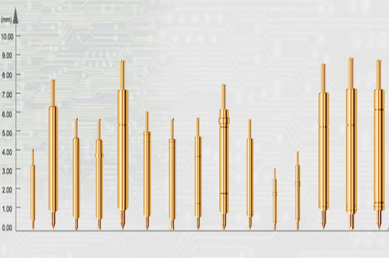
The semiconductor test probe is generally formed by the basic parts of the needle, needle tube, spring and so on after being riveted and pressed by the precision instrument. Because the size of the chip product is very small, the size of the probe is required to reach the micron level, and it is a high-end precision electronic component. The probe uses advanced manufacturing processes and materials to ensure high accuracy and stability.
The needle of the probe is made of high quality materials, such as brass, beryllium copper, which have excellent hardness, flexibility and corrosion resistance. At the same time, the probe is equipped with a precise spring structure, which can provide a stable contact force during the test process to ensure the accurate transmission of the test signal.

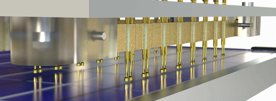
Semiconductor test probes are widely used in chip design verification, wafer testing and finished product testing. In the chip aging test, the probe realizes the precise connection between the chip pin or tin ball and the test machine by cooperating with the test machine, sorting machine, probe table and other equipment.
In the test process, the probe can accurately apply the input signal and collect the output signal, so as to judge whether the function and performance of the chip meet the design requirements.
In response to the continuous development of semiconductor technology, semiconductor test probes continue to innovate and break through in design and manufacturing. By optimizing the structural design, material selection and elasticity of the probe, Suntory improves the test accuracy and stability of the probe.
In addition, the probe uses advanced corrosion protection technology and surface gold-plating to enhance its electrical performance, stability and durability. These innovations not only extend the service life of the probes, but also improve test efficiency and reduce production costs.
With the continuous progress of semiconductor technology and the constant change of market demand.centalic Probe will pay more attention to innovation and breakthrough,To meet more complex and diverse testing needs. On the one hand, the probes will use more advanced materials and manufacturing processes, improving their accuracy and stability. On the other hand, the probes will also be combined with intelligent test equipment to achieve a more efficient and accurate test process.