Time:2024-08-28Reading:2672Second
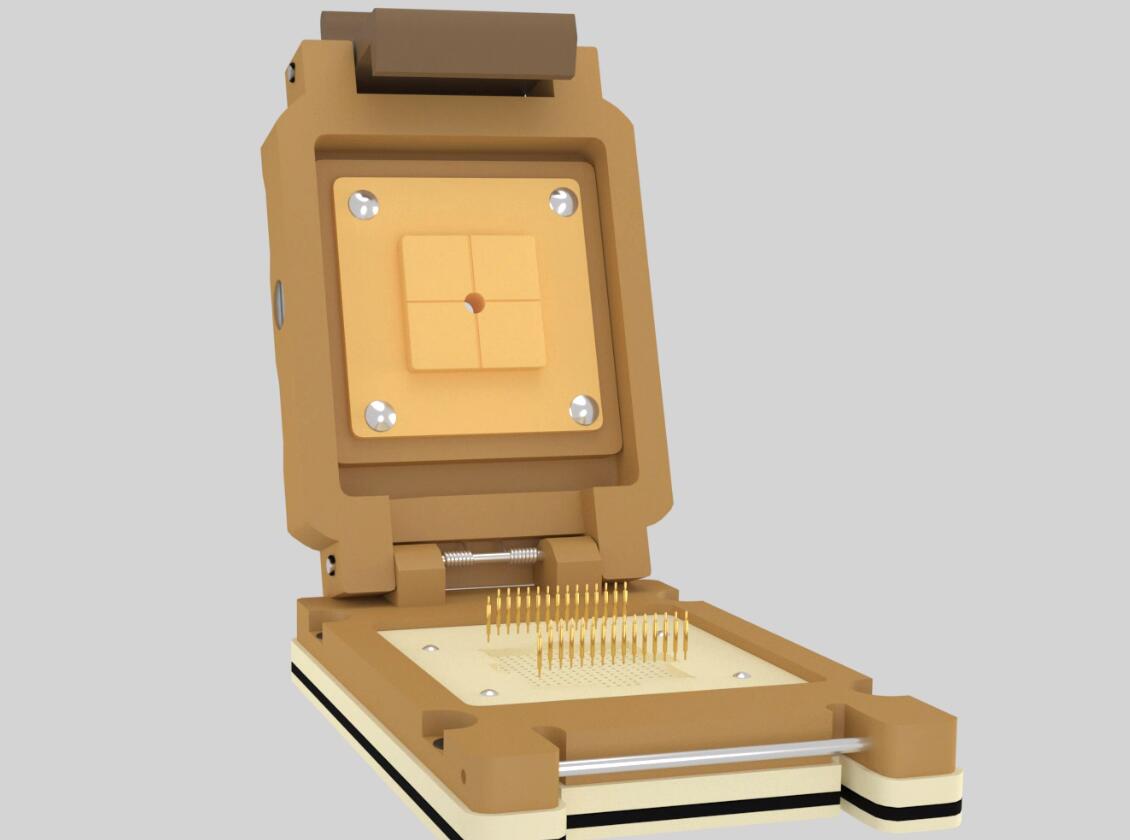
Semiconductor testing needles are mainly used in chip design verification, wafer testing, and finished product testing. They are the core components that connect chips, wafers, and testing equipment for signal transmission. By being used in conjunction with testing machines, sorting machines, and probe stations, they can screen for design defects and manufacturing defects in products. They have important value in ensuring product yield, controlling costs, guiding chip design, and process improvement. This sub industry is located in the middle of the semiconductor industry chain, with the upstream being metal processing and electroplating industries, and the downstream being chip design, wafer manufacturing, packaging and testing industries, playing an important role in quality control of semiconductor products.
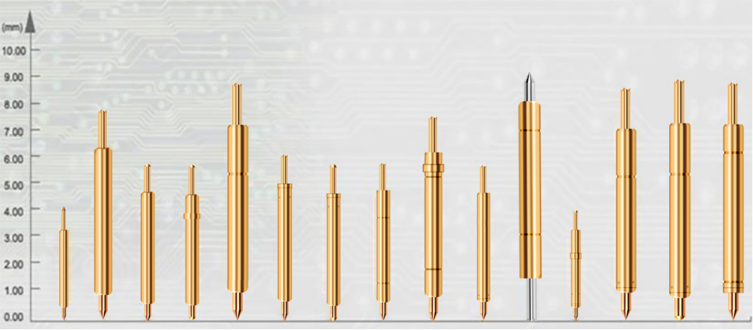
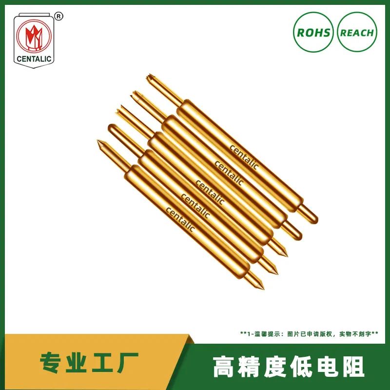
A probe is generally formed by riveting and pre pressing three basic components, namely a needle tip, a needle tube, a spring, and precision instruments. Its size requirement is to reach the micrometer level, making it a high-end precision electronic component with high manufacturing technology content. The appearance of probes for different purposes varies, but they generally have precision spring structures inside. The surface of the product is generally gold-plated, which has strong corrosion resistance, electrical performance, stability, and durability. As a key component in semiconductor testing equipment, the structural design, needle material, and elasticity of the probe all affect its stability, refinement, and signal transmission accuracy, thereby affecting the testing accuracy of the probe.
syringe needle:The selection of needle tip type in the testing environment also directly affects the testing effect. Needles are mainly made of materials such as brass, phosphor copper, beryllium copper, SK4, etc. Their hardness performance (brass<phosphor copper<beryllium copper<SK4), the higher the hardness, the more wear-resistant the needle.
Needle tube:Used for assembling needle bars, equipped with springs inside, mainly made of several materials such as phosphor copper tube, brass tube, white copper tube, etc.
Spring:Installed inside the needle tube to give the probe elasticity, the main materials are stainless steel wire and piano wire. Stainless steel wire is the preferred material for probe springs due to its corrosion resistance, high temperature resistance, and resistance to rusting; Qin steel wire has a strong elastic force value, but it is prone to rusting when damp, so there is generally no specific requirement to use Qin steel wire springs.
Surface coating of probe:The probe surface is plated with nickel, rhodium, and gold. Nickel plating and rhodium plating are more wear-resistant, while gold plating has the best electrical properties.
As a key component for semiconductor product testing, probes are located in the middle of the semiconductor industry chain in the manufacturing industry of testing equipment and its components. The upstream of the probe industry is the metal processing and electroplating industry, while the downstream is the chip design, wafer manufacturing and wafer foundry, packaging and testing industry. Semiconductor products that meet design specifications after testing are ultimately applied in many fields such as consumer electronics, automotive electronics, communication equipment, etc.

