Time:2024-10-10Reading:1718Second
The Importance of Probes
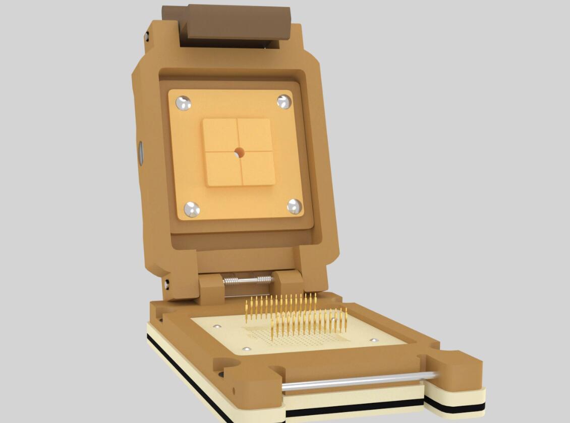
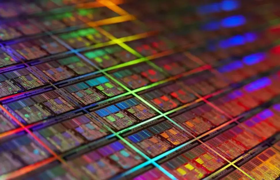
When it comes to probes, people may be unfamiliar with them, but the various electronic products we come into contact with in our daily lives, such as mobile phones, tablets, laptops, etc., are inseparable from them. The application of testing probes runs through all links of the entire electronic industry chain, from wafer inspection, chip packaging testing, integrated circuit testing, to various module testing. Quality inspection and product yield control in every link cannot be separated from testing probes.
Composition of probes
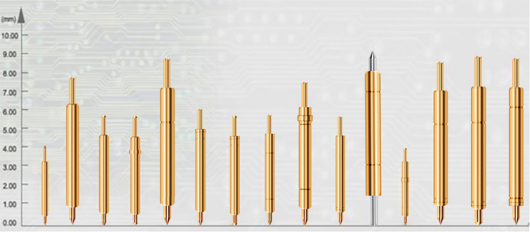
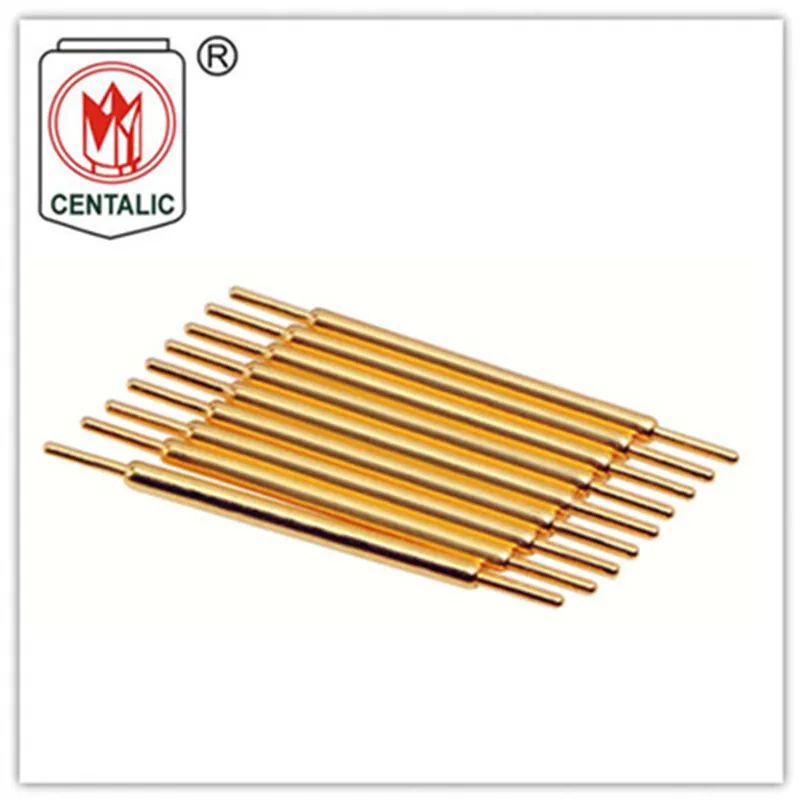
A probe is generally formed by riveting and preloading three basic components: a needle tip, a needle tube, and a spring with precision instruments.
syringe needle:The selection of needle tip type in the testing environment also directly affects the effectiveness of the test,Needles are mainly made of brass, phosphor copper, beryllium copperSeveral materials such as SK4.Their hardness performance(Brass<phosphor copper<beryllium copper<SK4), the higher the hardness, the more wear-resistant the needle will be.
Needle tube:Used for assembling needle bars, equipped with springs inside, mainly made of several materials such as phosphor copper tube, brass tube, white copper tube, etc.
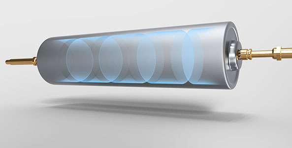
Spring:Installed inside the needle tube to give the probe elasticity, the main materials are stainless steel wire and piano wire. Stainless steel wire is the preferred material for probe springs due to its corrosion resistance, high temperature resistance, and resistance to rusting; Qin steel wire has a strong elastic force value, but it is prone to rusting when damp, so there is generally no specific requirement to use Qin steel wire springs.
Surface coating of probe:The probe surface is plated with nickel, rhodium, and gold.Nickel plating and rhodium plating are more wear-resistant, while gold plating has the best electrical properties.
Probe working principle
Due to the small size of semiconductor products, especially chip products, the size of probes is required to reach the micrometer level, which is a high-end precision electronic component with high manufacturing technology content.
During wafer or chip testing, probes are generally used for precise connection between wafer/chip pins or solder balls and the testing machine, to achieve signal transmission and detect performance indicators such as conductivity, current, functionality, and aging of the product.
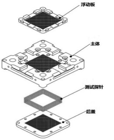
The appearance of probes for different purposes varies, but they generally have precise spring structures inside. The surface of the product is generally gold-plated, which has strong corrosion resistance, electrical performance, stability, and durability. As a key component in semiconductor testing equipment, the structural design, needle material, and elasticity of the probe all have an impact on its stability, refinement, and signal transmission accuracy, which in turn affects the testing accuracy of the probe.
Probe manufacturer
Due to the complex production process of semiconductor products, any process error can lead to a large number of product quality defects and have a significant impact on the performance of end use products. Therefore, choosing a good probe manufacturer is particularly important in semiconductor manufacturing. Centalic focuses on probe research and development production40For many years, we have had a complete "one-stop" production line. After the raw materials are received, they undergo turning, cleaning, and heat treatment---Electroplating - Assembly---Inspection and shipment, each process link is controlled by our company's self operated production line, with standardized production processes, strict control over delivery time and quality.
