Time:2025-03-07Reading:1355Second
In the world of chip manufacturing, any slight flaw can trigger the "butterfly effect" and bring down the entire product. As a key link to ensure product yield and cost control, the importance of chip testing is self-evident. The core purpose of chip testing is to ensure that the chip can accurately achieve all functions and performance indicators specified in the design specification under extremely harsh environments such as high temperature, low temperature and high humidity, as a basis for judging whether the chip meets the market access standards.
Entering the era of high-performance cpus, Gpus, Npus, DSPS and SoCs, the number of modules integrated inside chips has increased exponentially, and the number of failure modes in the manufacturing process has also increased, which makes the importance of chip testing increasingly prominent. The test probe, as one of the key components in the chip test process, plays an indispensable role behind the scenes. Next, let's delve deeper into the chip testing probe and uncover the mystery behind the micrometer-scale technology that underpins the chip industry's precision standards.

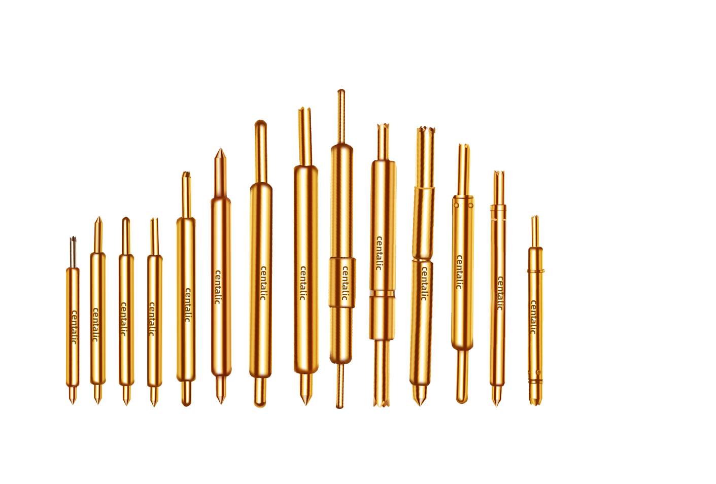
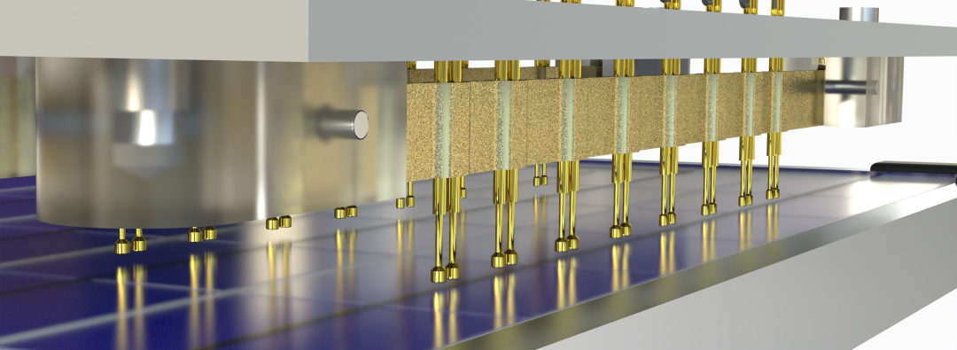
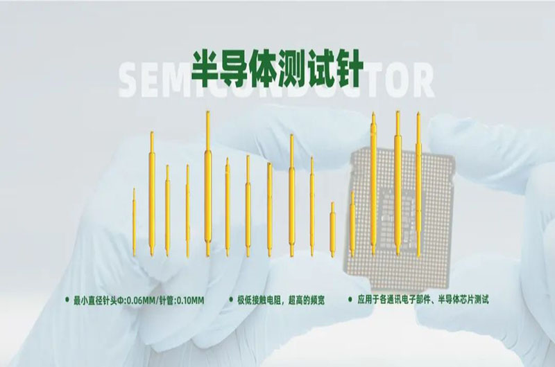
Chip manufacturing is a complex and precise process, from design to the flow sheet, and then to the package test, every step can not tolerate the slightest error. The test probe is the "gatekeeper" of the chip test link. They transmit electrical signals by touching the pad or pin of the chip to detect the electrical performance, functional integrity and reliability of the chip.

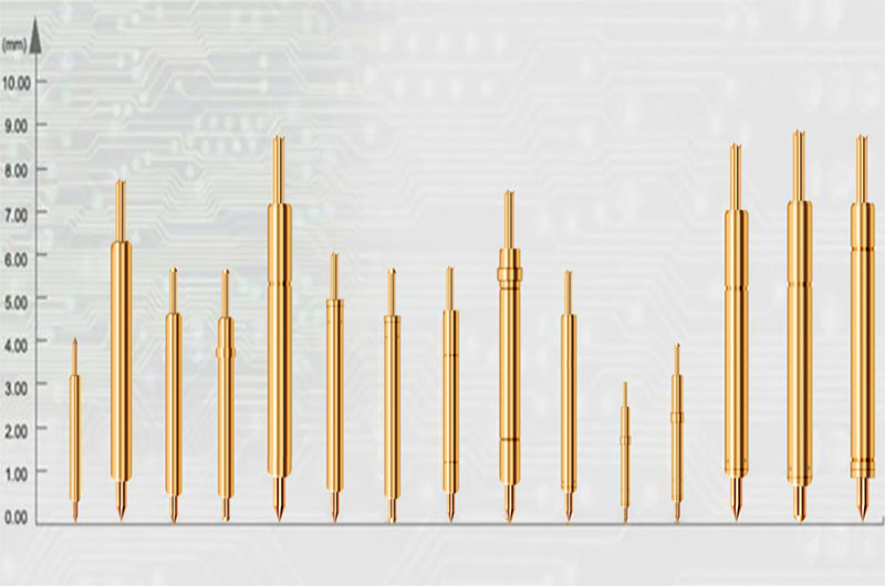
The essence of probe technology is its amazing precision and high reliability. As the chip manufacturing process continues to move toward smaller sizes, the contact points inside the chip, known as pads or bumps, become smaller and denser. In the case of chips with 7nm or even 3nm processes, the probe needs to achieve accurate contact in a narrow space of less than 100 microns, which puts nearly demanding requirements on the accuracy of the test probe. At the same time, in order to cope with the high frequency of test operations, the probe must also have sufficient durability to ensure that the stable performance is always maintained during the long, high intensity test process. To achieve the perfect combination of precision and durability, it is inseparable from the strong support of high-performance materials and precision manufacturing technology. High-performance materials give the probe good conductivity, wear resistance and stability, and precision manufacturing technology ensures the dimensional accuracy and structural stability of the probe, which complement each other and jointly achieve excellent performance of the probe.
The performance of the probe directly affects the efficiency and reliability of the chip test, and the rapid development of the chip industry continues to promote the progress of the probe technology, which shows a close symbiotic relationship.
Mover of Moore's Law: As chip manufacturing continues to shrink, probes need to adapt to smaller pad spacing and higher test frequencies. It can be said that the advancement of probe technology is an important support for the continuation of Moore's Law.
Challengers for emerging applications: In emerging fields such as 5G, artificial intelligence, and autonomous driving, the complexity and performance requirements of chips continue to increase, which brings new challenges and opportunities for probe technology.

Globally, the field of probe technology is extremely competitive. For a long time, companies from countries such as the United States, Japan and South Korea have firmly occupied the leading position in the market with their deep accumulation in precision manufacturing and materials technology. However, in recent years, Chinese companies have made great strides in the field of probe technology. centalic, for example, has been unswervingly committed to probe localization for more than 40 years, focusing on various types of test probe research and development and manufacturing of national high-tech enterprises. Through the use of advanced material structure, lean coating treatment and high-quality assembly process, the probe products developed by the company not only gradually approach the international advanced level in performance, but also have certain advantages in price, effectively reducing the cost of domestic chip manufacturing enterprises.

Future outlook: Intelligence and miniaturization of probes
Intelligent upgrades: Future probes may integrate more intelligent features, such as real-time data analysis and adaptive adjustment capabilities, to cope with complex and variable test needs.
Miniaturization and high density: As the chip process moves toward 2nm and even smaller nodes, the size and accuracy of the probe will also be further broken, and even single-atom level contact may be achieved.
Green manufacturing: Under the trend of environmental protection and sustainable development, the materials and manufacturing process of the probe will also pay more attention to green and low-carbon.

The probes, tiny as they are, are the guardians of the precision standards of the chip industry. They support every process of chip manufacturing with the ultimate technology and process to ensure that every chip can be in the best state to the market. In the rapid development of the chip industry today, the progress of the probe is not only the pursuit of technology, but also the promise of human life in the future. It is these small forces that converge into the mighty force that drives the giant wheel of science and technology forward.