Time:2025-02-10Reading:1052Second
On February 9th, according to domestic media reports, the United States has begun to implement new regulations on Chinese chip control, and has begun to block advanced processes below 16nm.
Previously, the Bureau of Industry and Security (BIS) of the US Department of Commerce issued two rules: one was to update export controls for advanced computing semiconductors, and the other was to include other entities from China (14) and Singapore (2) on the entity list.
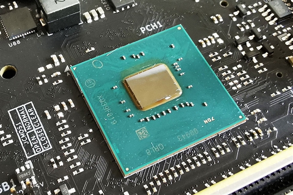
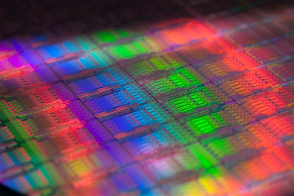
Among them, the applicable advanced logic integrated circuits are logic integrated circuits produced using "16nm/14nm node" and below processes, or using non planar transistor architectures. The United States will also strengthen due diligence on contract manufacturers and prevent their flow to China.
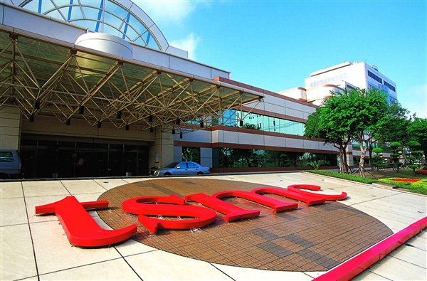
Under the implementation of the new regulations, TSMC has sent a formal notice to a large number of IC design companies in Chinese Mainland: from January 31, 2025, if the related products of 16/14nm and below are not packaged in the "approved OSAT" in the BIS white list, and TSMC has not received the certified signature copy from the packaging factory, the shipment of these products will be suspended.

A source familiar with the matter revealed that some mainland IC design companies have also been required to outsource the assembly, production, packaging, and testing of some sensitive orders, and IC design companies cannot intervene in the entire production process. This series of requirements undoubtedly poses significant challenges for mainland IC design companies.
From TSMC's recent actions, it can be seen that it is further actively cooperating with the US BIS to crack down on China's advanced process white gloves.
The suspension of shipments by TSMC has had a profound impact on mainland IC design companies and even the entire semiconductor industry.
In the short term, if the production plans of related companies are disrupted and delivery times are delayed, they not only face the risk of customer loss, but may also be at a disadvantage in market competition. At the same time, companies need to invest more time and cost in finding new packaging solutions and adjusting their supply chain layout.In the long run, this event will also force the semiconductor industry in Chinese Mainland to accelerate the pace of independent research and development and domestic substitution. On the one hand, mainland wafer fabs and packaging testing companies have ushered in development opportunities. On the other hand, chip design companies will also increase their research and development investment, explore more advanced chip design technologies, and reduce their dependence on advanced foreign processes and packaging.